Presentation Details
650V 4H-SiC VDMOS with Additional N Region_A Simulation Study
ID:2
View Protection:PUBLIC
Updated Time:2021-08-06 15:23:45
Hits:1545
Poster Presentation
Start Time:2021-08-27 13:05(Asia/Shanghai)
Duration:1min
Session:P Poster »
Abstract
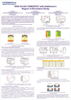
Aiming at the non-uniformity of channel length caused by two-layer lithography and high resistance of channel and JFET region in 4H-SiC VDMOS, a 650V 4H-SiC VDMOS with additional N-region is investigated. Sentaurus TCAD is utilized with the 4H-SiC material parameters included in the simulations to assess the threshold voltage Vth, on-state current IDS, forward drain source blocking voltage VDSS, maximum electric field in gate oxide EOX,max, doping profile and dimension of the proposed device.The variation rules of key electrical parameters and corresponding process conditions are revealed and compared with the 650V conventional 4H-SiC VDMOS. Simulation results demonstrate that the threshold voltage Vth of 650V VDMOS with additional N-region is 0.2V higher than that of conventional VDMOS, and the specific on-state resistance RDSon,sp of 650V VDMOS with additional N-region decreased by 0.8mΩ·cm2 compared with the conventional VDMOS when the VDSS and EOX,max satisfy the design value.
Keywords
4H-SiC;VDMOS;Additional N Region;JFET Resistance;Short channel
Speaker

Xiuxiu Gao
CORESING SEMICONDUCTOR TECHNOLOGY CO . LTDSubmission Author
All Comments
Important Date
-
Conference Date
Aug 25
2021
toAug 27
2021
-
Apr 21 2021
Abstract Submission Deadline
-
May 15 2021
Abstract Notification of Acceptance
-
Jun 25 2021
Final Paper Deadline
-
Aug 24 2021
Contribution Submission Deadline
-
Aug 27 2021
Registration deadline
Sponsored By
IEEE
IEEE ELECTRONIC DEVICE SOCIETY
IEEE ELECTRONIC DEVICE SOCIETY
Organized By
Huazhong University of Science and Technology
Contact Information
Previous Conferences
-
2025-08-15 China Beijing
2025 IEEE Workshop on Wide Bandgap Power Devices and Applications in Asia -
2025-08-15 China Beijing
The 2025 IEEE Workshop on Wide Bandgap Power Devices and Applications in Asia -
2023-08-27 Taiwan, China Hsinchu
2023 IEEE Workshop on Wide Bandgap Power Devices and Applications in Asia -
2018-05-17 China xian
IEEE Workshop on Wide Bandgap Power Devices and Applications in Asia

Submit Comment